Thursday - 20, November, 2014 (5:58 PM)
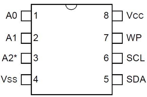
The 24FC1025 is a serial I2C EEPROM memory fabricated by microchip, it has 1024Kbits (128KB) of memory space and it is divided in two parts each one of 512Kbits (64KB); the first part goes from address 0x0000 to 0xFFFF and the second part goes from 0x10000 to 0x1FFFF.
Features:
- 128KB of memory space
- 2-Wire serial interface (I2C)
- Compatibility with 100 KHz, 400 KHz and 1.0 MHz clocks
- 2 hardware address bits allowing up to 4 devices on bus
- Hardware Write-Protect
- 128-Byte page write buffer (3ms typical)
- Operating voltage: 1.8V – 5.5V
Pinout PDIP:
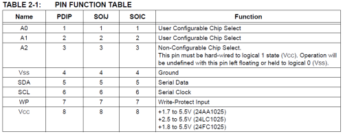
Pin function table:
Function block diagram:
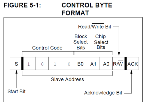
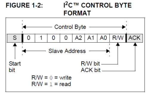
The control byte is composed by the static address (1010 = 0xA) plus the Bank select bit (It is 16th most significant address bit) plus the physical address on A1 and A0 pins (A2 pin cannot be used and it MUST be connected to VCC) and in the end the R/W bit as you can see in the image below:
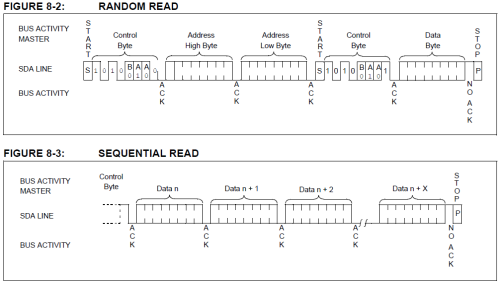
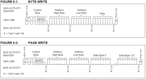
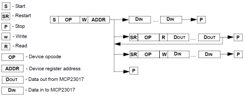
The I2C sequences to read or write a byte or page from this device are:
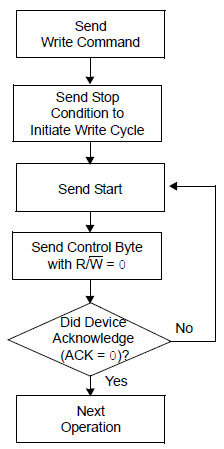
After sending a write command for a byte or a page the memory will start the writing cycle, while it is still busy we must not send another command. To know if the memory is busy or not you must send the same control command used for write and check the acknowledge bit, if acknowledge is received memory is not busy, otherwise it is still busy writing the data.
The below flow chart shows what was previously described above:
At this point you can see it is easy to read and write data to this memory so we will follow with an example.
The example consist on generating the values to rotate a led from bit 0 to 7 and backwards (0x01,0x02,0x04,0x08,0x08,0x04,0x02,0x01) and store these values into the first 8 Bytes of the memory (0x00000:0x00007).
Then generate values backwards to the first sequence (0x08,0x04,0x02,0x01,0x01,0x02,0x04,0x08) and save them in the first 8 Bytes of the second half of the memory (0x10000:0x10007).
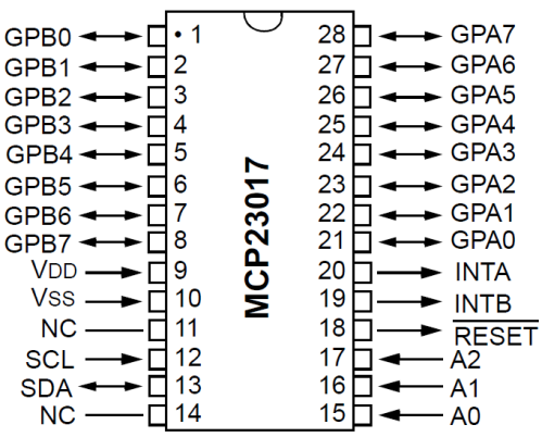
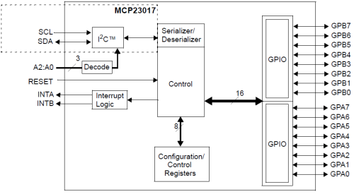
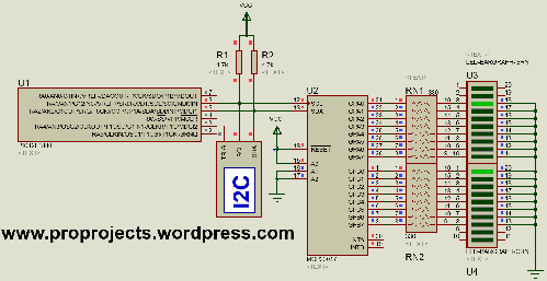
Next we are going to read each byte of the sequence and show it on a two 8b ports respectively, in the end we must see that one port is a mirror of the other. To do this I use the MCP23017 I/O Expander showing the first sequence on IOA and the other one in IOB.
/*
 *	Copyright (c) 2011-2014, http://www.proprojects.wordpress.com
 *	All rights reserved.
 *
 * 	Redistribution and use in source and binary forms, with or without modification,
 *	are permitted provided that the following conditions are met:
 *
 *	1.- Redistributions of source code must retain the above copyright notice,
 *          this list of conditions and the following disclaimer.
 *	2.- Redistributions in binary form must reproduce the above copyright notice,
 *          this list of conditions and the following disclaimer in the documentation
 *          and/or other materials provided with the distribution.
 *
 *	THIS SOFTWARE IS PROVIDED BY THE COPYRIGHT HOLDERS AND CONTRIBUTORS "AS IS" AND ANY
 *	EXPRESS OR IMPLIED WARRANTIES, INCLUDING, BUT NOT LIMITED TO, THE IMPLIED WARRANTIES
 *	OF MERCHANTABILITY AND FITNESS FOR A PARTICULAR PURPOSE ARE DISCLAIMED.
 *	IN NO EVENT SHALL THE COPYRIGHT HOLDER OR CONTRIBUTORS BE LIABLE FOR ANY DIRECT,
 *	INDIRECT, INCIDENTAL, SPECIAL, EXEMPLARY, OR CONSEQUENTIAL DAMAGES (INCLUDING, BUT NOT
 *	LIMITED TO, PROCUREMENT OF SUBSTITUTE GOODS OR SERVICES; LOSS OF USE, DATA, OR PROFITS
 *	OR BUSINESS INTERRUPTION) HOWEVER CAUSED AND ON ANY THEORY OF LIABILITY, WHETHER IN
 *	CONTRACT, STRICT LIABILITY, OR TORT (INCLUDING NEGLIGENCE OR OTHERWISE) ARISING IN ANY
 *	WAY OUT OF THE USE OF THIS SOFTWARE, EVEN IF ADVISED OF THE POSSIBILITY OF SUCH DAMAGE.
 */

/*********************************************************************
 * By:              Omar Gurrola
 * Company:         https://proprojects.wordpress.com
 * Processor:       PIC12
 * Compiler:        XC8 v1.32
 * File Name:       main.c
 * Created On:      July 27, 2014, 10:38 AM
 * Description:
 * ~~~~~~~~~~~~~~~~~~~~~~~~~~~~~~~~~~~~~~~~~~~~~~~~~~~~~~~~~~~~~~~~~~~~
 * Rev.     Date        Comment
 * 1.0      07/27/14    Initial version
 *********************************************************************/

/** INCLUDES *******************************************************/
#include "pic12f1840_cbits.h"  // Apropiate configuration bits header
#include "main.h"
#include "pic12f1840_i2c.h"
#include "mcp23017.h"
#include "m24fc1025.h"

/** DEFINES ********************************************************/

/** PROTOTYPES *****************************************************/
#define SetClockTo32Mhz()  OSCCONbits.IRCF = 0b1110; OSCCONbits.SPLLEN = 1
void delay_ms(uint16_t);

/** GLOBAL VARIABLES ***********************************************/

/** CODE DECLARATIONS ****************************************/
void main(void) {
    SetClockTo32Mhz();

    delay_ms(1000); // Wait for proteus to load simulation

    i2c_init(I2C_SPEED_STANDARD_100KHZ);
    m24fc1025_init(0b00);
    mcp23017_init(0b001); // Init MCP23017 with the address 001
    mcp23017_write_reg(MCP23017_REG_IODIRA, 0x00); // IOA configure as output
    mcp23017_write_reg(MCP23017_REG_IODIRB, 0x00); // IOB configure as output

    // Write first 16 Bytes of memory
    uint32_t addr = 0;
    for (uint8_t c = 0x01; addr < 8; c = c << 1, addr++) { // Rotate bit
        m24fc1025_write_byte(addr, c);
        while (m24fc1025_is_write_busy()); // Wait for write to finish
    }
    for (uint8_t c = 0x80; addr < 16; c = c >> 1, addr++) { // Rotate bit to the other side
        m24fc1025_write_byte(addr, c);
        while (m24fc1025_is_write_busy()); // Wait for write to finish
    }

    // Write on the address 0x1000+ 16 Bytes of memory
    uint32_t addr = 0;
    for (uint8_t c = 0x80; addr < 8; c = c >> 1, addr++) { // Rotate bit
        m24fc1025_write_byte(addr + 0x1000, c);
        while (m24fc1025_is_write_busy()); // Wait for write to finish
    }
    for (uint8_t c = 0x01; addr < 16; c = c << 1, addr++) { // Rotate bit to the other side
        m24fc1025_write_byte(addr + 0x1000, c);
        while (m24fc1025_is_write_busy()); // Wait for write to finish
    }

    for (;;) {
        // Read data and write it to IOA
        for (uint32_t addr = 0; addr < 16; addr++) {
            mcp23017_write_reg(MCP23017_REG_GPIOA, m24fc1025_read_byte(addr)); // Write to IOA
            mcp23017_write_reg(MCP23017_REG_GPIOB, m24fc1025_read_byte(addr + 0x1000)); // Write to IOB
            delay_ms(250); // Wait some ms between cycles
        }
    }
}

void delay_ms(uint16_t t_ms) {
    for (t_ms; t_ms > 0; t_ms--) {
        for (uint16_t c = 886; c > 0; c--);
    }
}
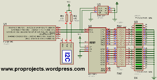
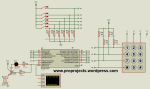
Below you can see the schematic of the example simulated on proteus.
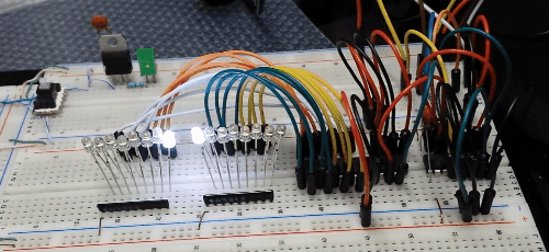
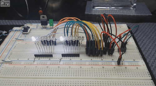
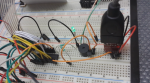
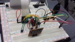
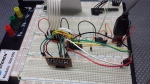
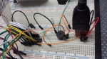
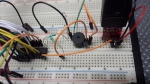
The circuit was armed on the breadboard and it is working as expected.
Well that’s all for today, happy programming and until next time.
References:
- I2C Info, “I2C Bus Specification”, 2014, http://i2c.info/i2c-bus-specification
- Robot Electronics, “Using the I2C Bus”, 2014, http://www.robot-electronics.co.uk/acatalog/I2C_Tutorial.html
- Microchip, “MCP23017/MCP23S17 16-Bit I/O Expander with Serial Interface”, 2007, http://ww1.microchip.com/downloads/en/DeviceDoc/21952b.pdf
- Microchip, “24AA1025/24LC1025/24FC1025 1024K I2C Serial EEPROM”, 2013, http://ww1.microchip.com/downloads/en/DeviceDoc/20001941L.pdf